General Description
The RTQ2538H is a high-current, ultra-low noise, ultra low-dropout (LDO) linear regulator. This document explains the function and use of the RTQ2538H evaluation board (EVB) and provides information for the setup and operating instructions, a schematic diagram, a printed circuit board (PCB) layout, and a bill of materials (BOM). For more detail information, please refer to the RTQ2538H datasheet.
Performance Specification Summary
The RTQ2538H Evaluation Board (EVB) is a four-layer board measuring 50mm x 33.5mm with a copper thickness of 1oz, and the Table 1 is the summary of the EVB performance specificiaiton.
Table 1. RTQ2538H Evaluation Board Performance Specification Summary
|
Key Features
|
Test Conditions
|
Min
|
Typ
|
Max
|
Unit
|
|
Input Range
|
|
Input Voltage
|
|
1.1
|
1.1
|
6.5
|
V
|
|
Enable Input Voltage
|
|
1.1
|
--
|
6.5
|
V
|
|
Output Range
|
|
Output Voltage
|
Using external resistive voltage divider
|
0.8
|
0.8
|
5.5
|
V
|
|
Line Regulation
|
IOUT = 1mA, 1.1V ≤ VIN ≤ 6.5V
|
--
|
0.05
|
--
|
%/V
|
|
Load Regulation
|
1mA ≤ IOUT ≤ 2A
|
--
|
0.08
|
--
|
%/A
|
|
Dropout Voltage
|
VIN = 1.1V to 6.5V, IOUT = 2A,
VFB = 0.8V - 3%
|
--
|
34
|
90
|
mV
|
|
Package
|
|
WQFN-12L 2.2x2.5 (FC)
|
Power-up & Measurement Procedure
Suggestion Required Equipments:
- RTQ2538H evaluation board
- DC power supply capable of at least 6.5V and 2A
- Electronic load capable of 2A
- Function generator
- Oscilloscope
Test Procedure with Suitable Measurement Equipment:
- Connect input power supply with wide and short as possible to VIN and GND through GP1/GP2 terminals.
- Connect the electronic load to VOUT and GND through GP3/GP4 terminals.
- Turn on the power supply and make sure that the input voltage does not exceeds 6V.
- Check output voltage regulation with different IOUT for normal operation.
Notifications:
- Do not turn on input power supply before all connections are ready.
- Do not use the oscilloscope probe with long ground lead for output ripple voltage measurement, it is recommended to touch the probe tip and groundring directly across the last output capacitor.
Detailed Description of Hardware
Headers Description and Placement
Carefully inspect all the components used in the EVB according to the following Bill of Materials table, and then make sure all the components are undamaged and correctly installed. If there is any missing or damaged component, which may occur during transportation, please contact our distributors or e-mail us at evb_service@richtek.com.
Test Points
The EVB is provided with the test points and pin names listed in the table below.
|
Test Point
|
Pin Name
|
Description
|
|
GP1
|
VIN
|
Positive terminal for supply input voltage.
|
|
GP2
|
GND
|
Negative terminal for supply input voltage.
|
|
GP3
|
VOUT
|
Positive terminal for output voltage.
|
|
GP4
|
GND
|
Negative terminal for output voltage.
|
|
GP5
|
GND
|
Reference ground test point.
|
|
TP1
|
VIN
|
For supply input voltage measurement.
|
|
TP2
|
EN
|
Enable voltage input pin.
|
|
TP3
|
PGOOD
|
For power good measurement.
|
|
TP4
|
VOUT
|
For output voltage measurement.
|
|
JP1
|
Enable
|
Connection for Enable voltage.
|
|
JP2
|
PGOOD
|
Connection for power good pu-ll high voltage.
|
Bill of Materials
|
Reference
|
Count
|
Part Number
|
Description
|
Package
|
Manufacturer
|
|
U1
|
1
|
RTQ2538HN-TA
|
Linear Regulator
|
WQFN-12L 2.2x2.5 (FC)
|
RICHTEK
|
|
C3, C6
|
2
|
1210X476K160CT
|
Capacitor, Ceramic,
47µF, 16V, X5R
|
C-1210
|
WALSIN
|
|
C4, C5
|
2
|
0603B104K500CT
|
Capacitor, Ceramic,
0.1µF, 50V, X7R
|
C-0603
|
WALSIN
|
|
C9, C11
|
2
|
0603B103K500CT
|
Capacitor, Ceramic,
10nF, 50V, X7R
|
C-0603
|
WALSIN
|
|
C10
|
1
|
0603B105K250CT
|
Capacitor, Ceramic,
1µF, 25V, X5R
|
C-0603
|
WALSIN
|
|
R1
|
1
|
RTT031182FTP
|
Resistor, Chip,
11.8k, 1%
|
R-0603
|
RALEC
|
|
R2
|
1
|
WR06X3741FTL
|
Resistor, Chip,
3.74k, 1%
|
R-0603
|
WALSIN
|
|
R3, R5
|
2
|
WR06X1003FTL
|
Resistor, Chip,
100k, 1%
|
R-0603
|
WALSIN
|
Typical Applications
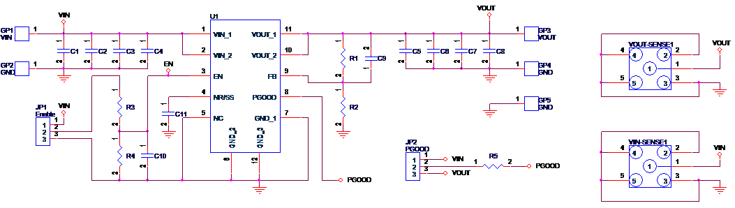
EVB Schematic Diagram
Measure Result
|
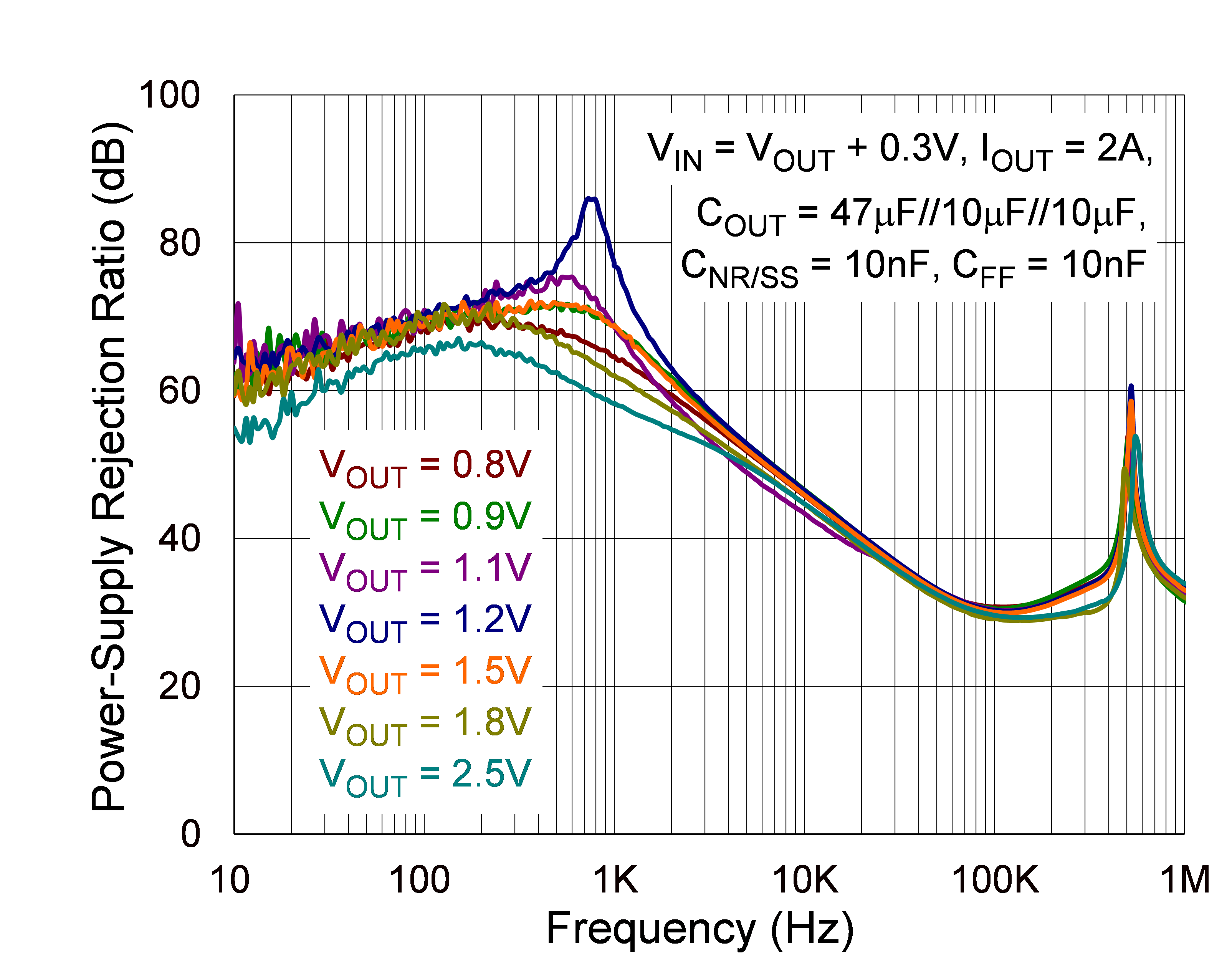
PSRR vs. Frequency and VOUT
|
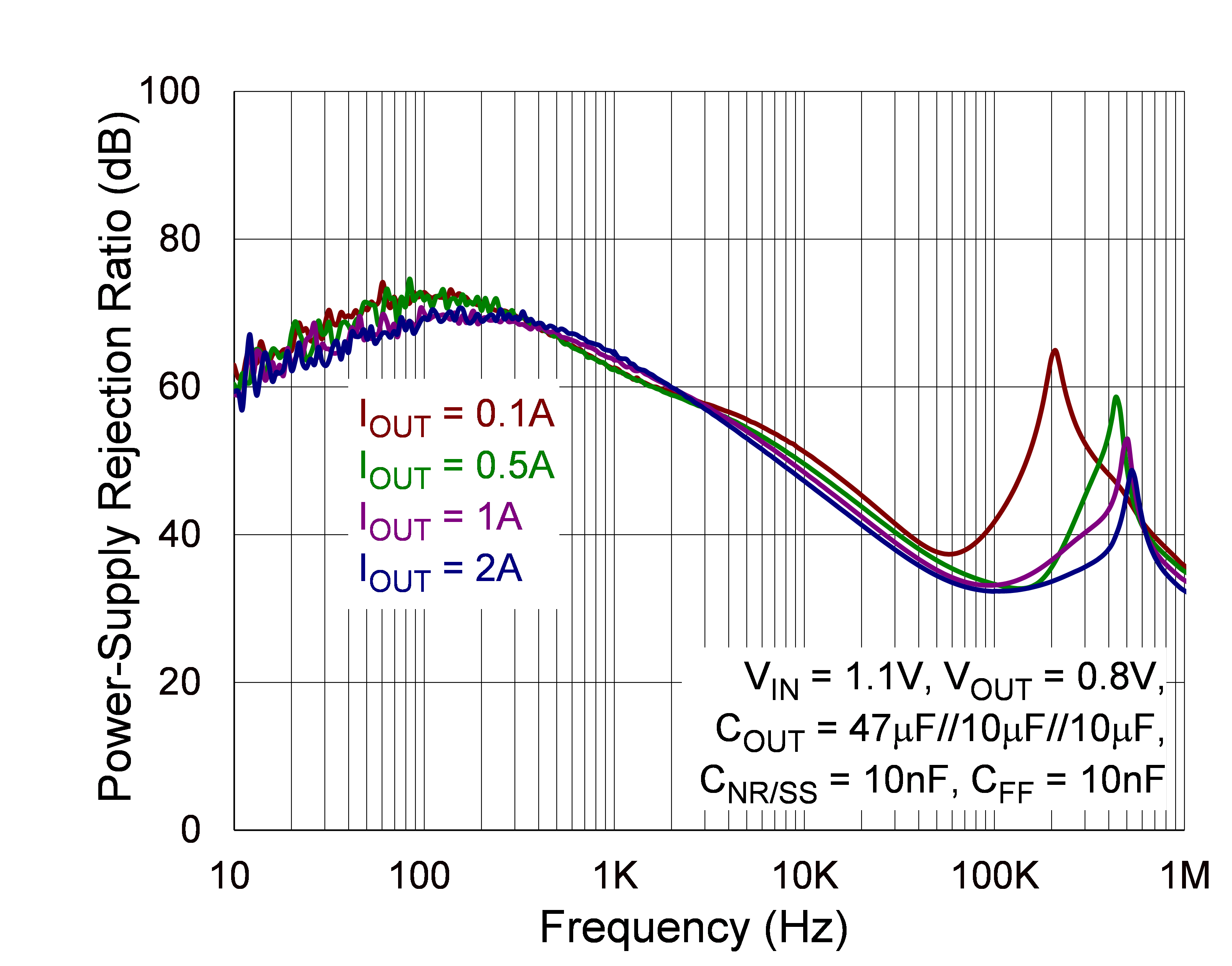
PSRR vs. Frequency and IOUT
|
|
|
|
|
Output Noise vs. Frequency and VOUT
|
Output Noise vs. Frequency and CNR/SS
|
|
|
|
|
Power Up Response
|
Load Transient Response
|
|
|
|
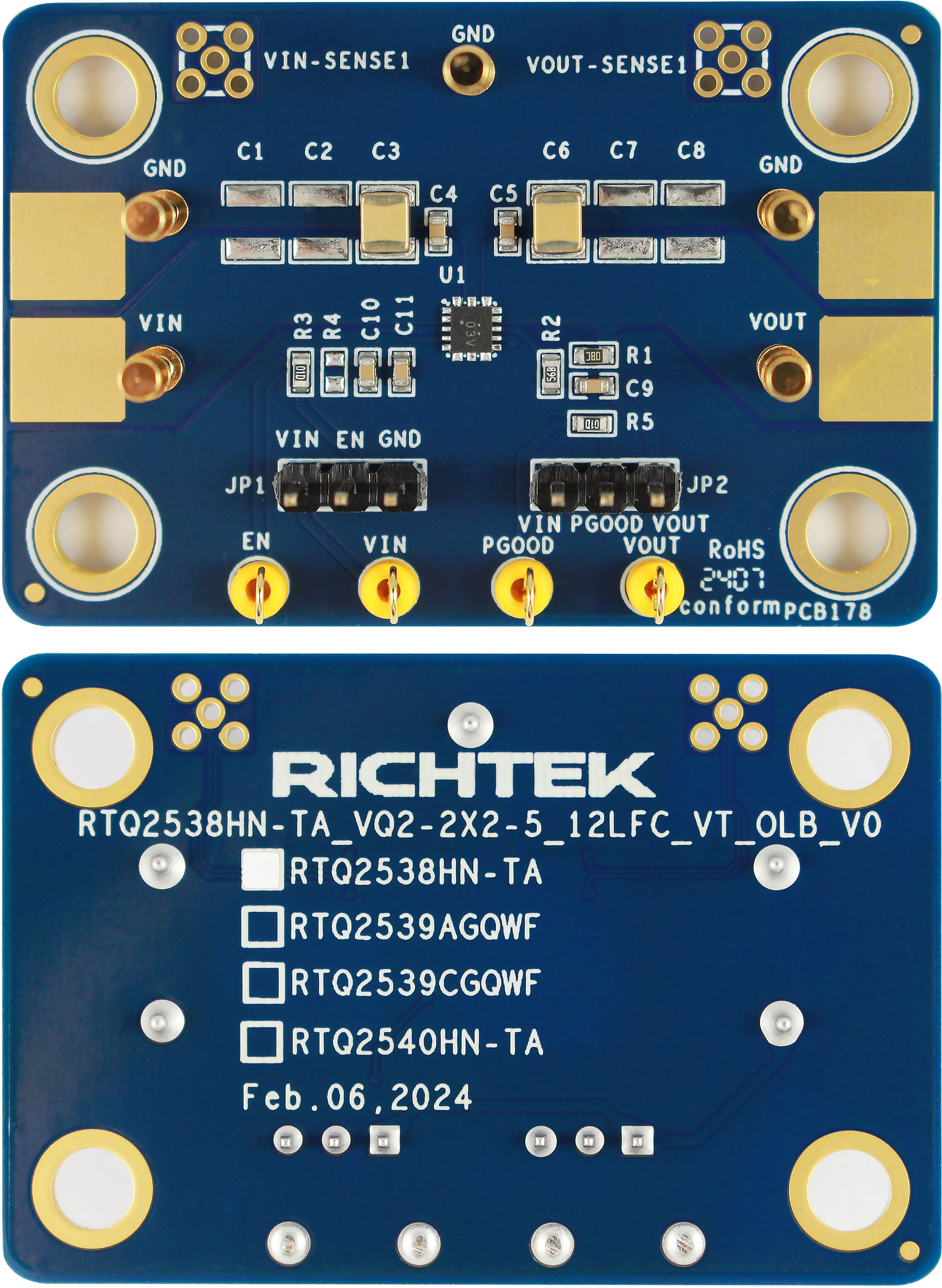
Evaluation Board Layout
Figure 1 to Figure 4 are the RTQ2538H evaluation board layout.
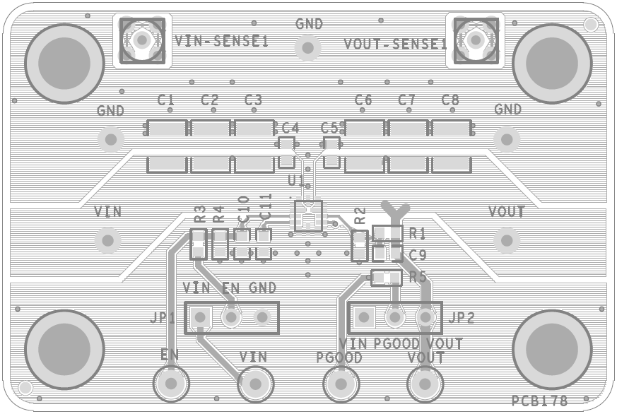
Figure 1. Top View (1st layer)
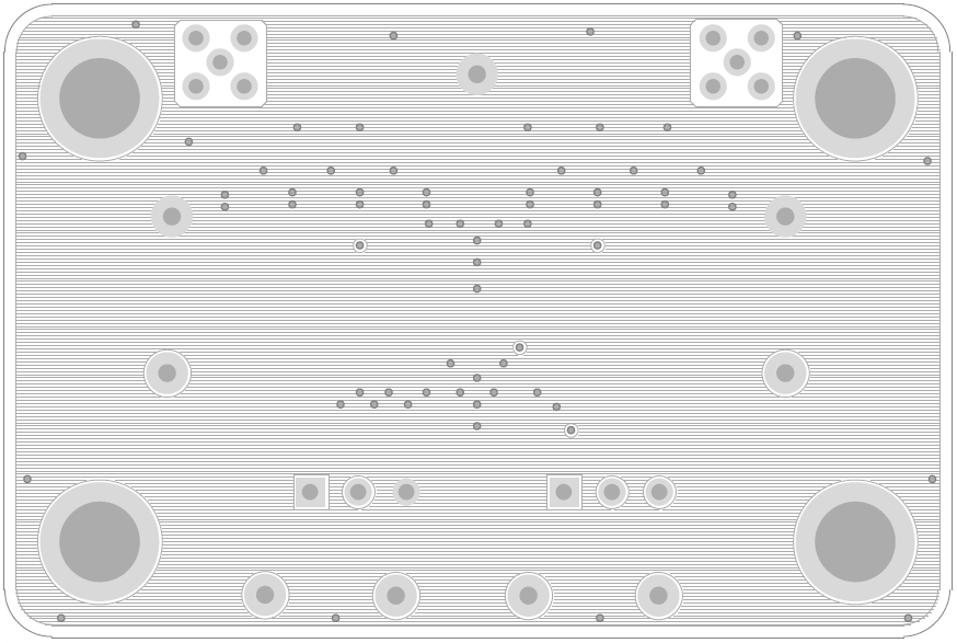
Figure 2. Inner Side (2nd Layer)
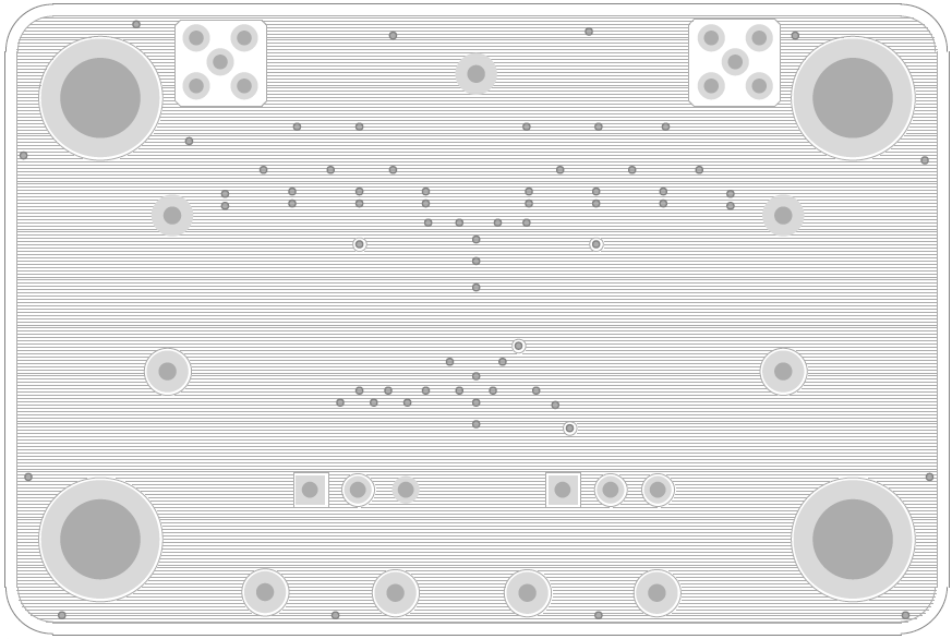
Figure 3. Inner Side (3rd Layer)
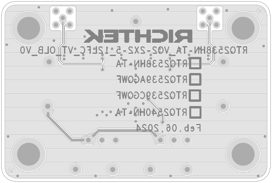
Figure 4. Bottom View (4th Layer)